
Researchers at IBM have detailed methods that could let chip designers move away from silicon transistors to smaller – and faster – carbon nanotubes.
For most of the last five decades, the processing hearts of all our computers, game consoles, smartphones, cars, media players and even alarm clocks have been made of silicon. No surprise: The namesake of Silicon Valley is cheap, readily available, and easily manipulated during manufacturing processes.
But scientists and researchers now believe silicon-based processors are reaching their limits. Physical laws limit how small silicon transistors can get before the signals they process just become a random electrical haze. That’s why new research from scientists at IBM seems to hold so much promise for the future of computing: They may have found a realistic way to ditch silicon in favor of carbon nanotubes.
Carbo-nano-what?

Carbon is one of the most versatile elements in nature, taking the form of everything from coal to pencil lead and diamonds. One of the forms it can take is graphene. You can think of graphene as a bit like molecular chicken wire: individual carbon atoms bond together in a hexagonal pattern, forming a sheet that can be just one atom thick. At a very basic level, a carbon nanotube is a sheet of graphene that’s rolled up and joined with itself to form a cylinder: The hexagonal structure of the carbon bonds means that tube can ideally be seamless — no point is weaker than any other — and the tubes can be very, very long — molecularly speaking, anyway. Carbon nanotubes have been constructed that are more than 100 million times longer than they are wide. Sure, that’s still tiny to you and me, but carbon nanotubes can be far larger than any other known cylindrical nanostructure — and that’s a tremendously useful characteristic if you’re trying to design very tiny things like processor chips.
Like silicon, carbon nanotubes are also semiconducting, and (in some cases, in theory) can be more than 1,000 times more conductive than copper. This makes them one of the very few nano-materials that could feasibly be used to replace silicon in chip design.
Creating order from chaos
Chip designers looking to use carbon nanotubes for processors face one major problem: how to manipulate them and lay them out in the kinds of tiny, very precise patterns needed for processors. Current chip manufacturers essentially create wafers of silicon embedded between layers of non-conductive material, then use chemicals or lasers and particle beam etching to trace out paths and individual transistors.
Transistors are the absolute heart of digital processors, acting at the gates that control the individual ones and zeros (or bits) that define digital technology. A single character in the most basic email message or text takes seven bits (or transistors) to represent; a single pixel in a digital photograph requires over 500 bits. Transistors are responsible for both memory (like RAM and flash storage), but (by switching on and off again to transform and manipulate data) for all execution and code running on a device.
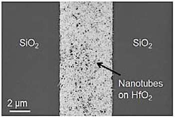
The old-school etching approaches to making transistors wouldn’t work with nanotubes, but researchers at IBM came up with a new technique, reported in Nature Nanotechnology. First, the researchers made a traditional wafer, but with a layer of hafnium deposited on silicon. Next, they put the carbon nanotubes in a chemical that made them soluble in water. Finally, they dipped the hafnium wafer in the solution of nanotubes, then dipped the wafer in a second chemical that sticks to the hafnium and acts as a two-part epoxy to bind the nanotubes — but only to the areas of the wafer with exposed hafnium. The result? Carbon nanotubes neatly lined up on paths etched in a wafer — just the sort of thing you’d want for a chip. The IBM team was able to make both memory and microprocessor chips with more than 10,000 working transistors.
How tightly packed are the nanotubes? About one billion nanotubes per square centimeter. According to IBM materials scientist (and study co-author) James Hannon, the technique deposited one nanotube roughly every 150 to 200 nanometers. That’s not small enough for a realistic microprocessor, and it’s a far cry from 22 nanometer distances that have been used by memory manufacturers since 2008 (and which are currently mainstream in Intel’s Ivy Bridge processors), but Hannon told the BBC that represents a 100-fold improvement over previous efforts to pack nanotubes into chip-like configurations — and puts the technology within striking distance of silicon.
Nanotubes might power your future

Processors built using carbon nanotubes could be the breakthrough that enables digital technology to continue advancing at a steady pace. Since the development of the first integrated circuit in 1958, the number of transistors chipmakers have been able to cram into the same are has been doubled roughly every two years — a maxim known as Moore’s Law, named for Intel co-founder Gordon Moore. When Moore first articulated the idea back in 1965, nobody really thought the industry would be able to sustain that pace for long. Yet despite a few hiccups, engineers and researchers have largely been able to maintain that pace through innovations in chip manufacturing processes (like Intel’s “3D” tri-gate transistors and exotic new materials). The first integrated circuits contained only a few transistors; today, mainstream chips like Intel’s Ivy Bridge line carry as many as 1.4 billion.
Silicon hasn’t reached the end of the road yet; chipmakers already have the next generation or two of silicon chips planned out. After the current 22nm process, expect to see 14nm chips — switches are getting so small they can be meaningfully measured in individual atoms. That sets a startlingly high bar for the plants that make them, which would have to execute near atom-accurate operations billions of times for every single processor they produce. On the other hand, the techniques outlined by IBM’s nanotube research point toward self-assembling solutions where molecules wind up in the proper placed through chemical reactions.
In theory, processors built around carbon nanotubes could be considerably smaller than today’s transistor technology. Just like today’s processors, smaller means they consume less power. That means less heat and far longer battery life for mobile devices. Furthermore, the electrical properties of carbon nanotubes also means they can switch on and off faster than silicon-based transistors, meaning they could operate at significantly higher clock speeds than today’s chips. That’s a good thing: While Moore’s Law is still in force for transistor density, processor clock speeds have started to plateau in recent years, with chipmakers getting more performance out of chips by adding additional processor cores rather than making those cores run faster. Carbon nanotube processors could theoretically handle speeds as high as 8GHz or 9GHz and run at half or one third the power of today’s chips – at least in rough calculations.
So nanotube processors would be smaller, faster — and since they’re made of carbon, they’d be greener, right? Probably not. Although carbon nanotubes are certainly less damaging to the environment than many compounds and materials used in high-tech products, the process of manufacturing carbon nanotube processors isn’t likely to be inherently greener than making silicon wafers — and don’t expect the devices they power to be magically biodegradable.
Similarly, the chips will still be difficult to make and expensive. Just like today’s chips, the newest, fastest versions will only power the newest, flashiest, high-end devices — but those devices could be much smaller than today’s gizmos. For instance, with the iPhone 5 Apple has packed more processing power into a handset than it ever put into a PowerPC-based notebook. Extend trends like that, and you start to see tablets that only a few millimeters thick, technology that might be able to support things like bendable and flexible portable devices and wearable computing technology like Google Project Glass - with enough processing power to handle speech recognition, augmented reality, multitasking and high-end graphics — and batteries that last for days or even weeks.
When will they be on sale?
Carbon nanotube processors might prove to be the future of computing … but it’s going to be a long while before they appear retailer’s shelves. The process outlined by IBM still has to be considerably refined to make it practical in the real world. Assuming that can be done, existing chip manufacturing facilities will have to be converted to use the new processors, or (as likely) whole new chip fabrication facilities will have to be built. All in all, we’re probably looking at at least another decade before the technology is commercially viable. But, conveniently, that’s just about when silicon will probably hit the end of its feasible development.
[Images via Shutterstock / imredesiuk, Wikimedia Commons / AlexanderAlUS ]
Source : digitaltrends[dot]com


Post a Comment